PCB manufacturing technology
Every year we invest heavily in the best PCB manufacturing technologies. In order to meet our customers’ expectations for quality, reliability, flexibility, innovation and speed.
We make customized PCBs in sophisticated hi-tech production plant in Boskovice.
Take a look at the facilities in which your PCBs are manufactured.
Any questions?
Do you want more info?
CAM software
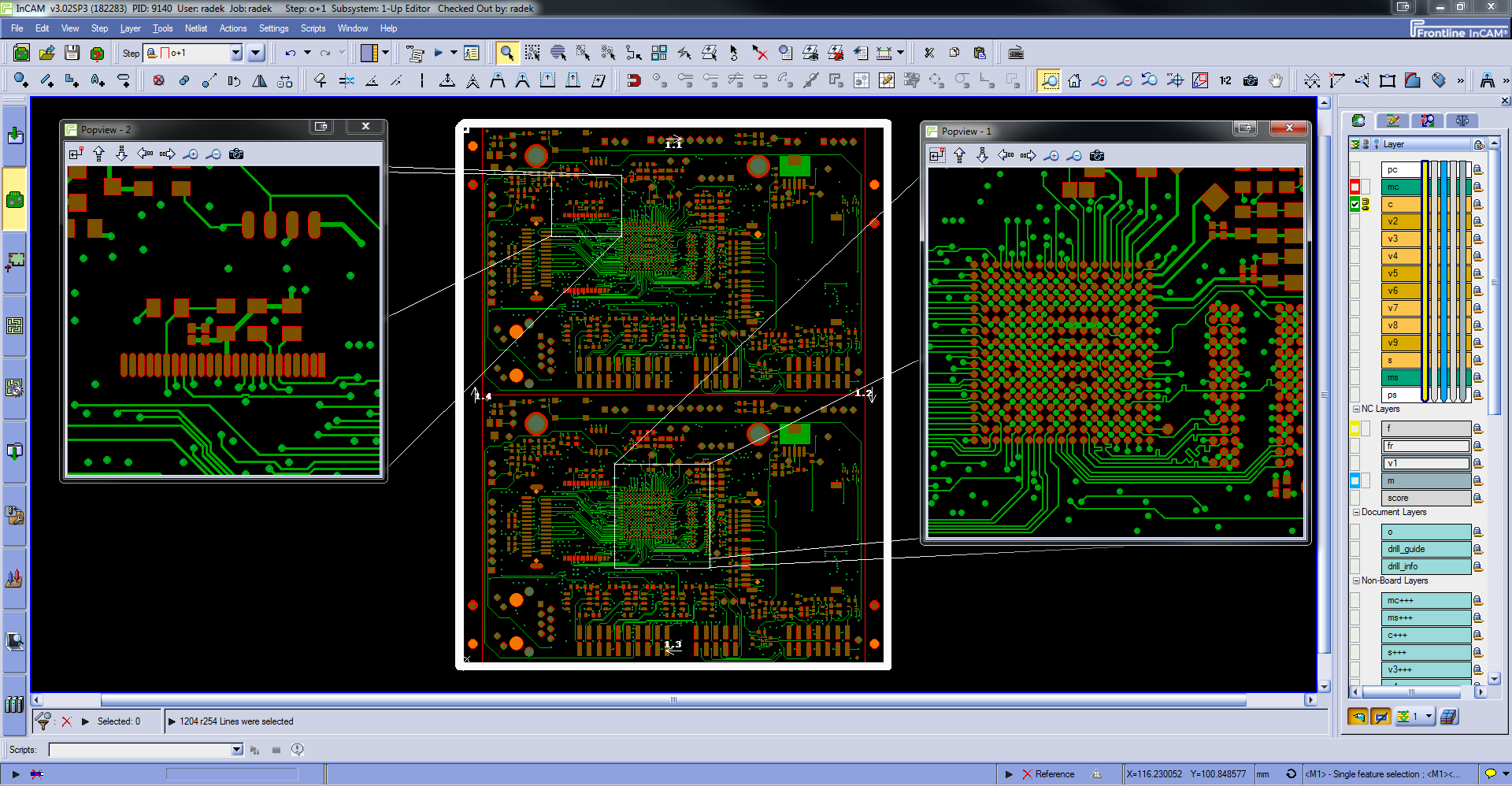
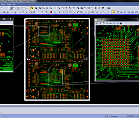
InCAM

InCam is a superior CAM system from Orbotech for data processing for printed circuit boards manufacturing. Its modular structure allows optimisation of data processing particular steps with ODB++ format support. InCAM software is a very powerful tool surpassing competitive CAM software in many ways. Parallel running of more processes in the background, possibility of cooperative processing by more users at the same time or 64-bit structure able to utilize multicore processors are its key properties. DFM analyse function increases speed and efficiency of data processing and together with wide scale of optimising modules it represents top tool for HDI printed circuit board processing. Its indispensable advantage is direct connection to equipment for direct exposure, photo plotter and AOI optical tester.
CNC
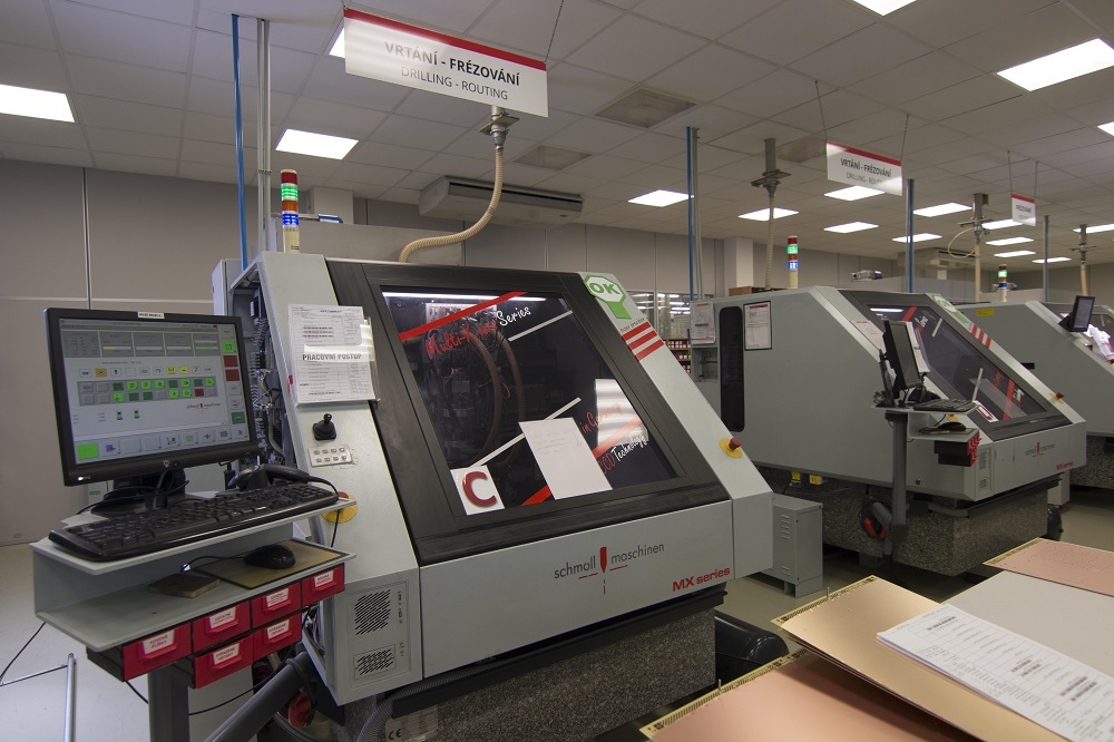
Schmoll - CNC drilling and routing
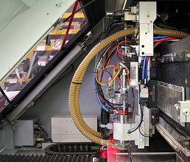
SCHMOLL A-MX1-300DH-CCD is two-spindle drilling machine with one drilling table and automatic loader, linear motors and controlled Z axis, registration by CCD camera.
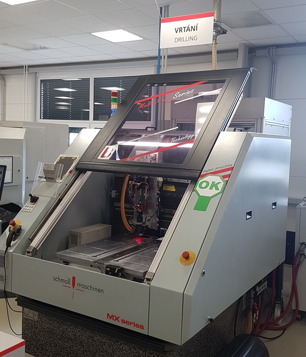
Schmoll - CNC drilling
SCHMOLL A-MX1-200S-CCD is single-spindle drilling machine with one drilling table and automatic loader, linear motors and controlled Z axis. Registration of innerlayers is provided using CCD camera system.
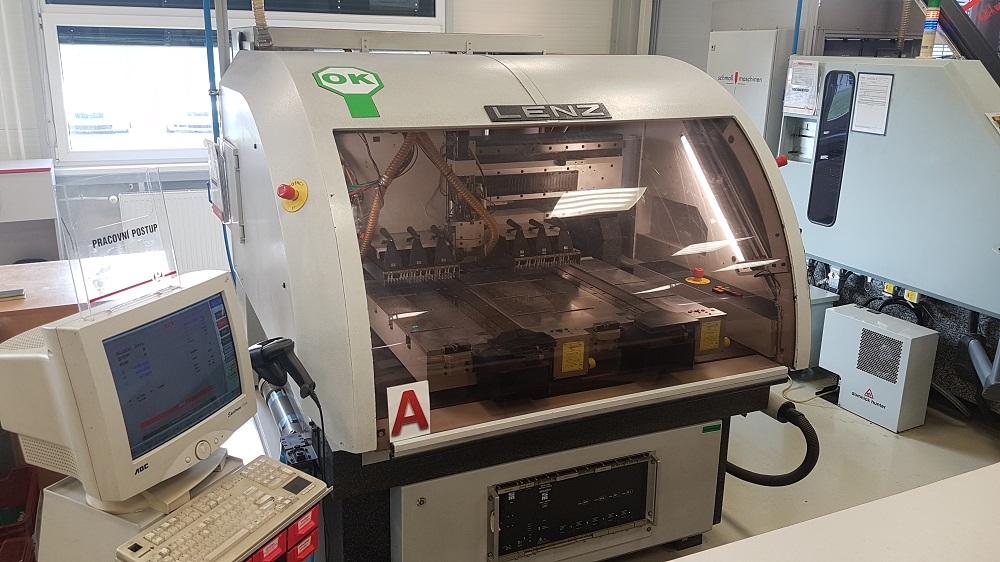
LENZ - CNC drilling

LENZ DLG 460-2-AL is two-spindle drilling machine with automatic loader, linear motors and controlled Z axis.
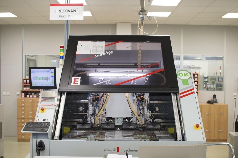
Schmoll - CNC drilling and routing

SCHMOLL LM2 is two-spindle drilling machine with one drilling table and automatic loader, linear motors and controlled Z axis. It allows drilling of PCB and routing it to final dimensions.
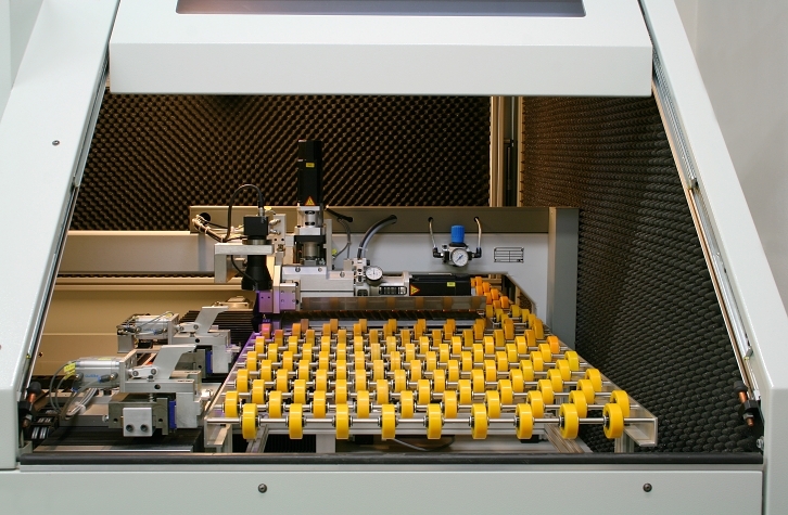
LHMT - V-scoring
LHMT SCM411 scoring machine is equipment for printed circuit V-scoring. This machine is furnished with CD camera for ideal setting of grooving program with produced board.
Clean Room
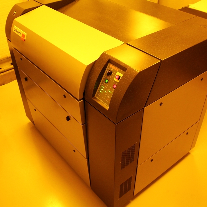
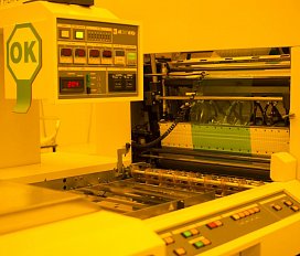
Orbotech - photo plotter
LP-9008 is a modern laser photo plotter from Orbotech able to draw on films motives with 25 400 DPI resolution, which in practice means minimum line width 20 µm.
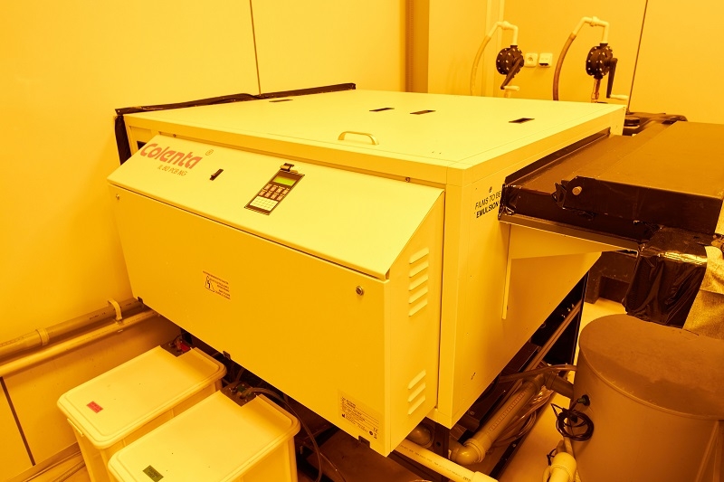
Colenta - film processor
Highly reliable device for processing of film patterns.
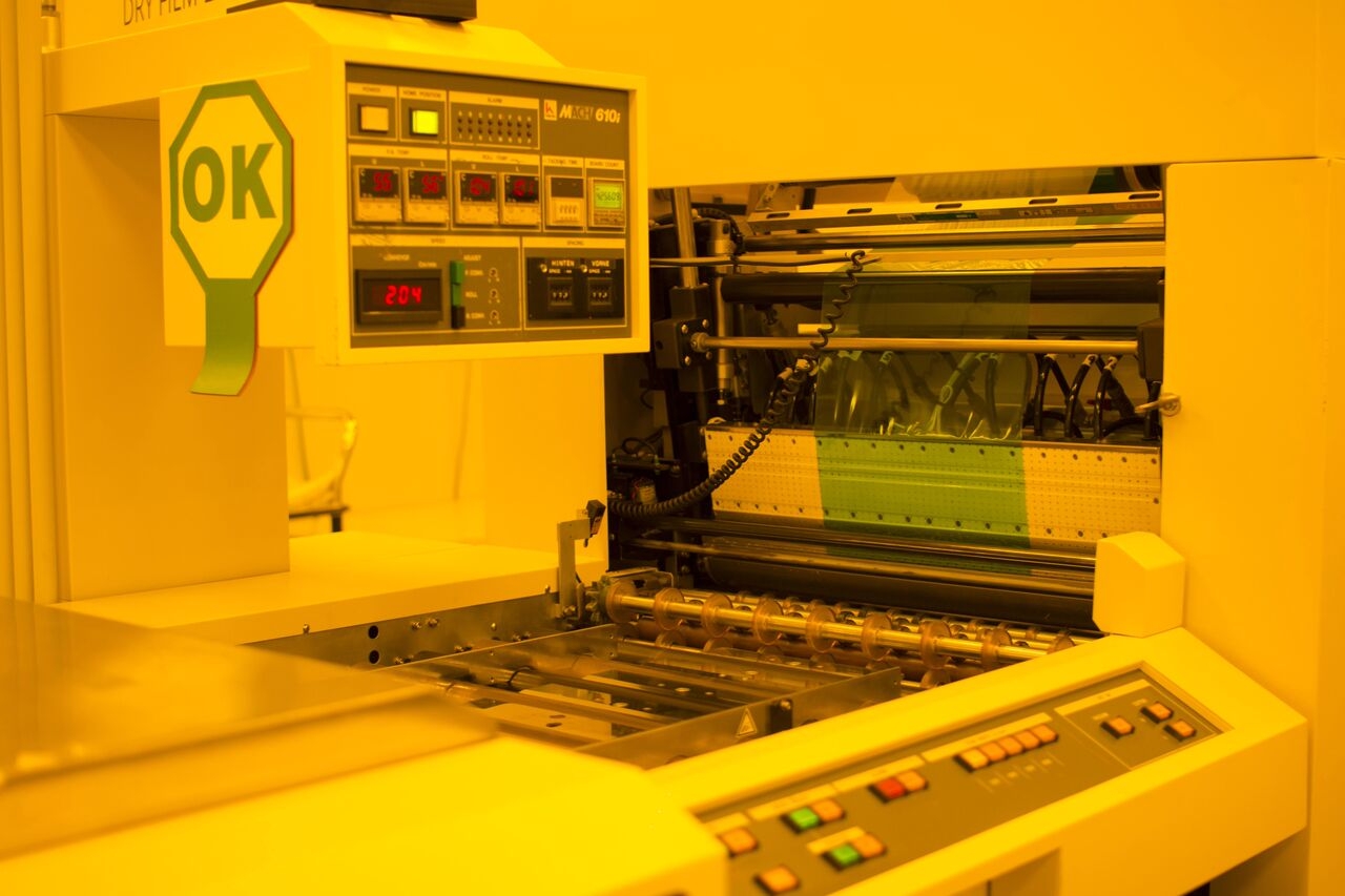
Hakuto - dry resist laminator
Hacuto Mach 610i machine dispose of automatic panel detection function and is also equipped for flexible materials lamination. Lamination process ensures flawless photoresist application on PCB´s surface.
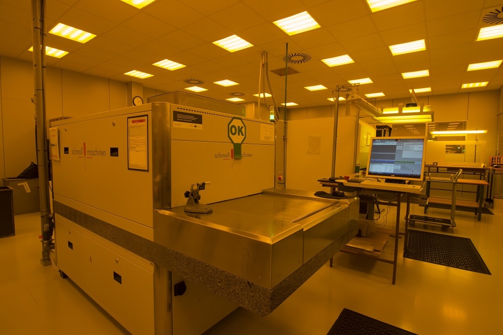
Schmoll - MDI -TT direct imaging

Using MDI (Micromirror Digital Imaging) we are able to create the PCB motive directly on the dry resist without using a film master. The source of radiation is LEDs that emit radiation at 365, 375, 395 and 405 nm wavelengths. By selecting the appropriate wavelengths of radiation, the optimum parameters for creating the motive can be set not only for the resist but also for the solder mask.
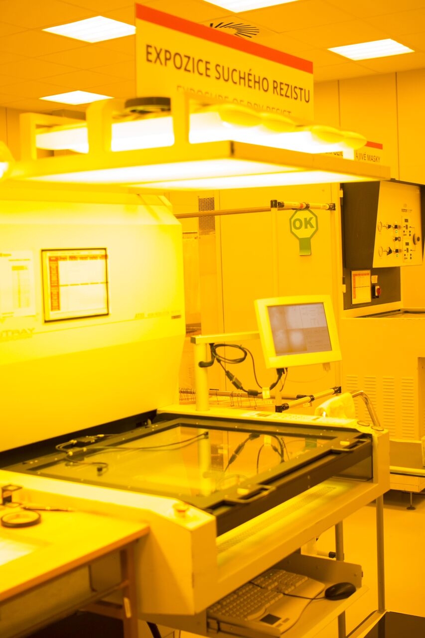
Olec - expozition of solder resist
OLEC brand is leader among producers of systems for image transfer for printed circuits. OLEC Accutray AT30 with automatic registration of films and automatic guidance allow processing of even highly complex PCB.
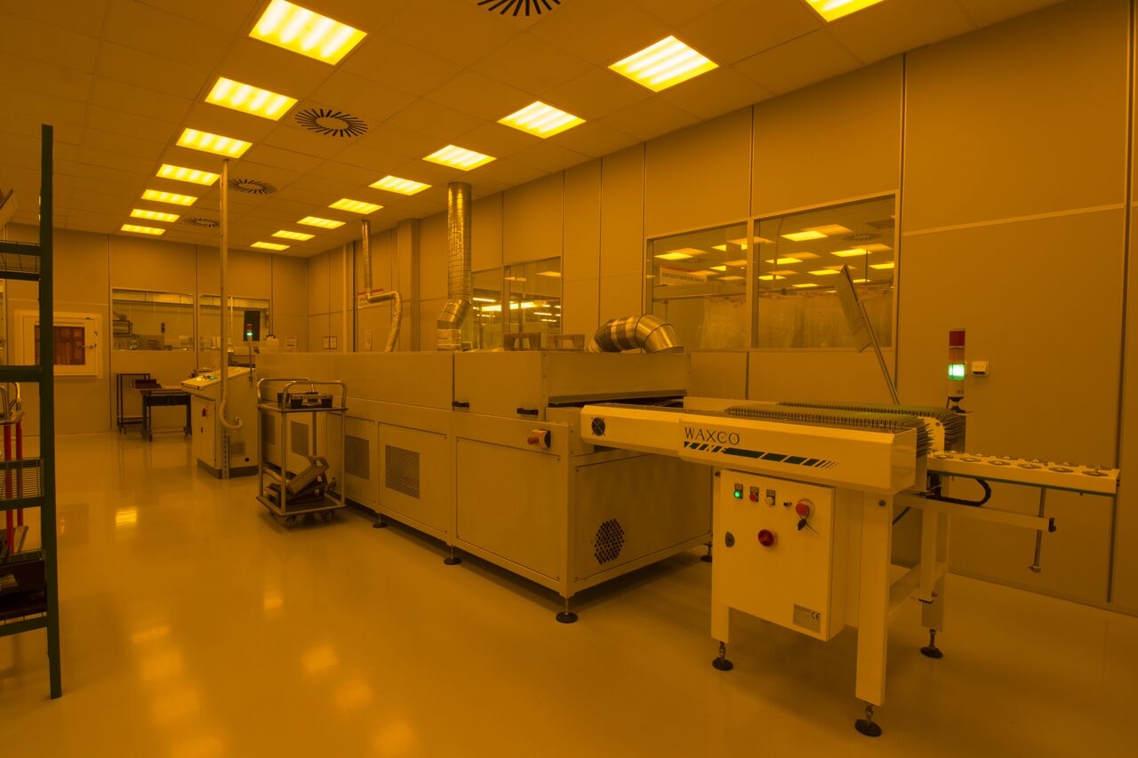
Bürkle - curtain coting
Automated curtain coating equipment with temperature and viscosity controlling of solder mask resist and thus providing solder mask constant thickness and continuous process. Placement of pre-drying oven in-line immediately behind the curtain coating machine give us the maximum productivity of solder mask application process.
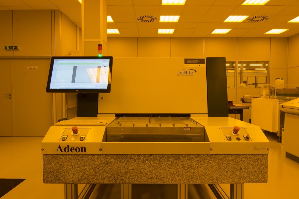
JetRite - digital legend printing
Substitution of traditional screen printing. This technology allows printing directly on PCB surface using ink heads. Letter minimal thickness is 130um.
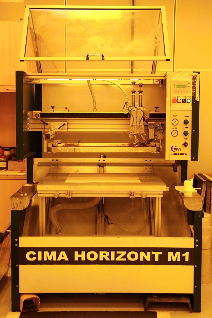
Cima Zlín - screen printing
Horizon M1 semi-automatic screen printer with work plate horizontal lifting. The equipment is designed directly for PCB screen printing.
Wet processes
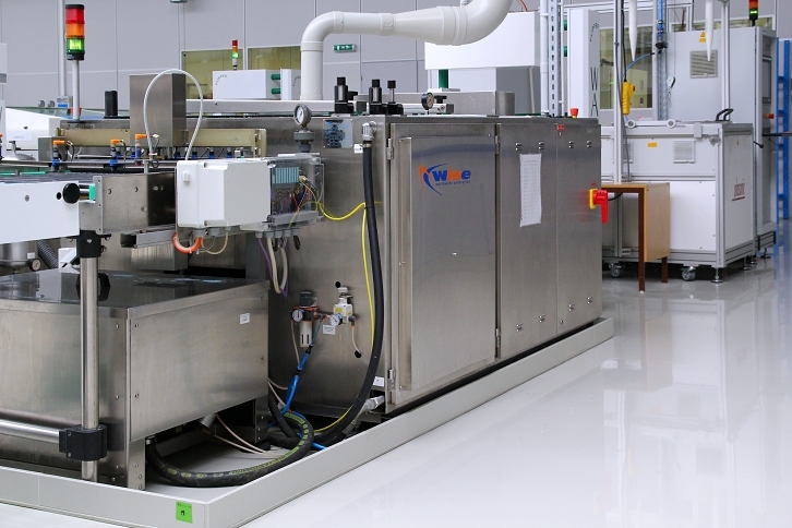
WISE - brushing
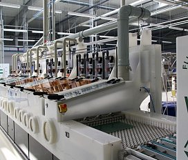
Within the PCB production a brushing line is used for removal of burr from holes and oxidation from copper surfaces. The line is equipped with an automatic brush pressure setting and high pressure rinsing. Of course there is a filtration system for brushes and rinses.
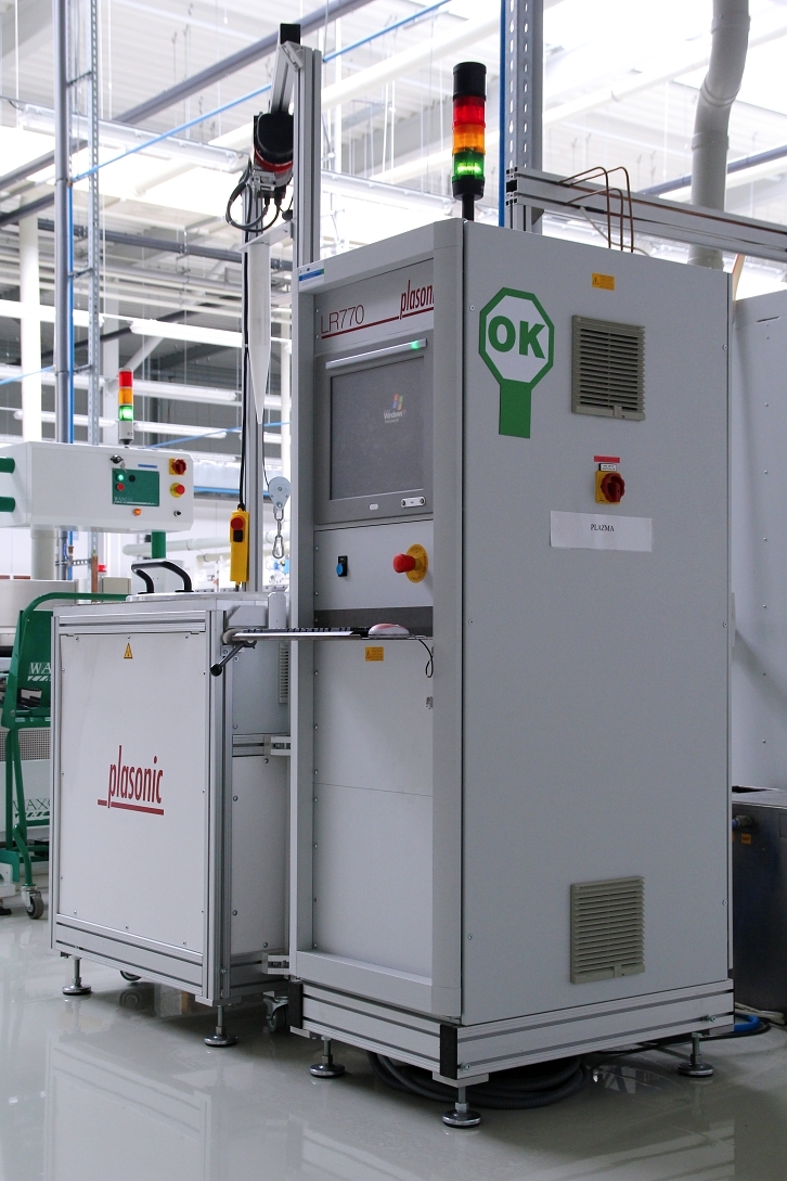
Plasonic - plasma
Plasma treatment removes resin from walls of drilled holes to allow perfect connection of galvanic copper on PCB internal layers. This method is convenient either for standard FR4 materials and for advanced materials with higher Tg, halogen free, polyimide (flex, rigid-flex), PFE etc. as well
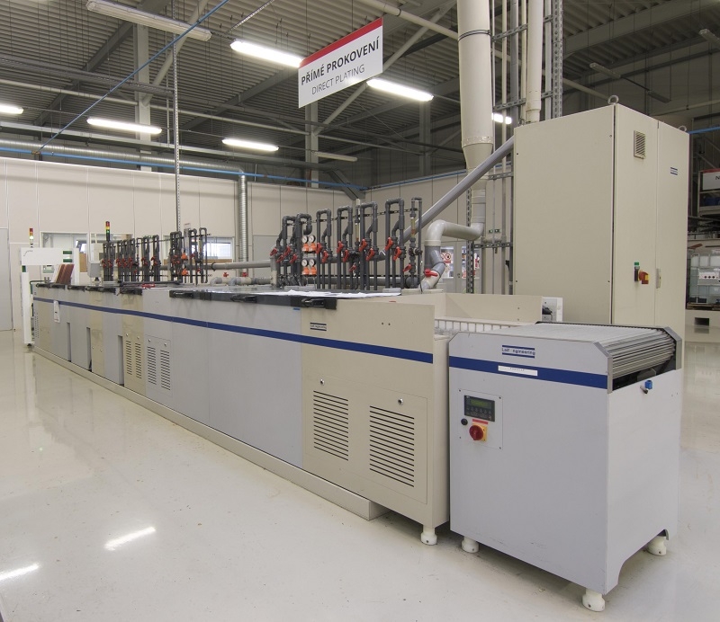
Laif - direct plating
The process of direct plating is based on graphite layer deposit on PCB dialectric surface which are to be plated through with galvanic copper. It is essential process verified by long-term operation.
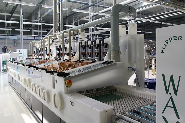
Matusewitz - chemical cleaning
Matusewitz MECetch line – this process replaces the brushing process in some areas. Matusewitz MECetch line – this process replaces the brushing process in some areas. It brings far greater copper roughness and therefore it´s bigger surface. This treatment is suitable for application with dry resist, solder mask even for finishes pre-treatment. This technology is used also for copper surface treatment for flexi PCBs thanks to its minimal mechanical stress. Modern line software enables flexible program setting and simultaneously controls the automatic dosing based on continuous copper measurement.
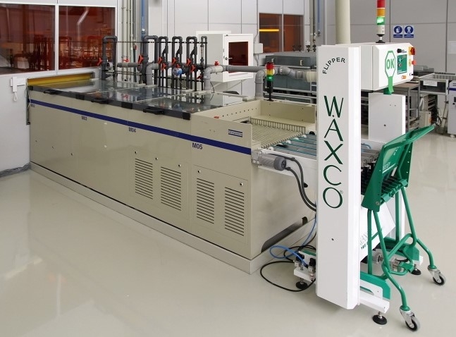
Laif - resist developer
After dry resist exposure future connections are developed. This means that not imaged areas of photo sensitive material are chemically removed in sodium carbonate solution.
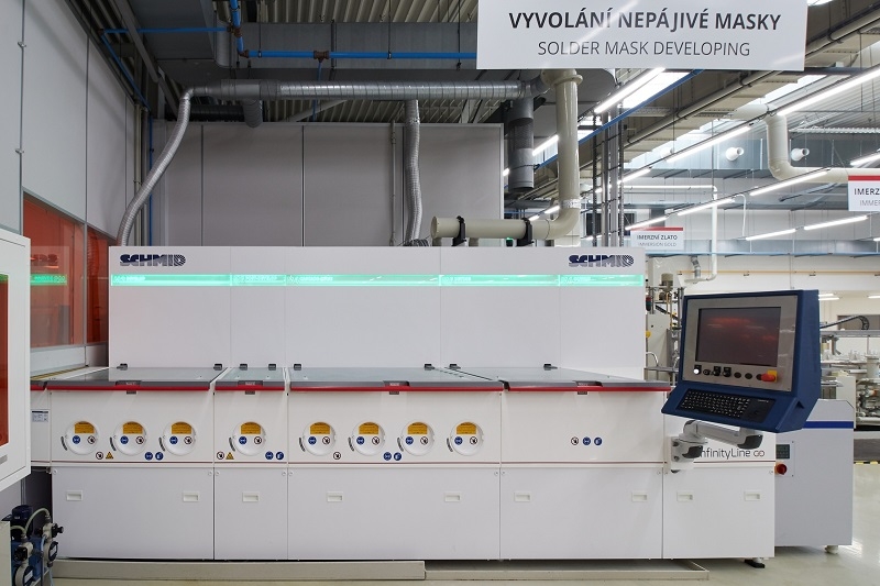
Schmid - solder mask developer
Not imaged surfaces of solder mask are removed by developing process. These are the places to which the customer can later solder.
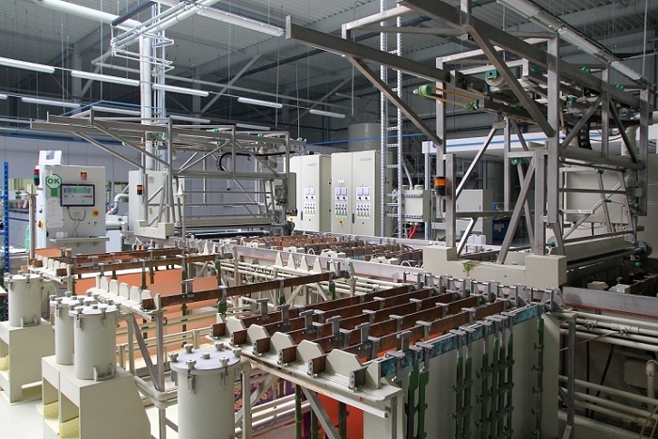
PPT Trenčianská Teplá - galvanic line
Galvanic line serves for plating-through of holes and copper thickening to required thickness and it represents core process of PCB production. The line contains acid copper and galvanic tin baths.
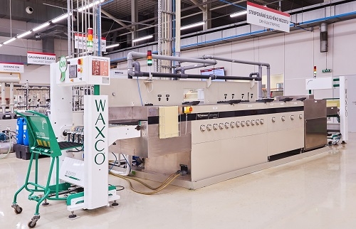
Wise - dry resist stripper
The new line, from the Italian company WISE, is equipped with an automatic mode of control and dosing of chemicals.
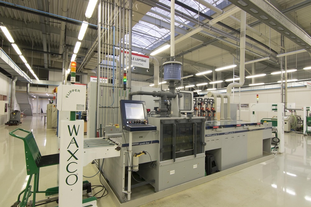
Schmid - acid etching
Excess copper is removed from PCB by using copper dichloride solution. The system itself measures bath selected parameters and upon results adds necessary chemicals.
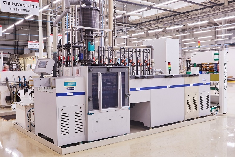
Laif - alcalic etching

Ammoniacal etchant removes excess copper from PCB. The process itself controls solution pH value and density.
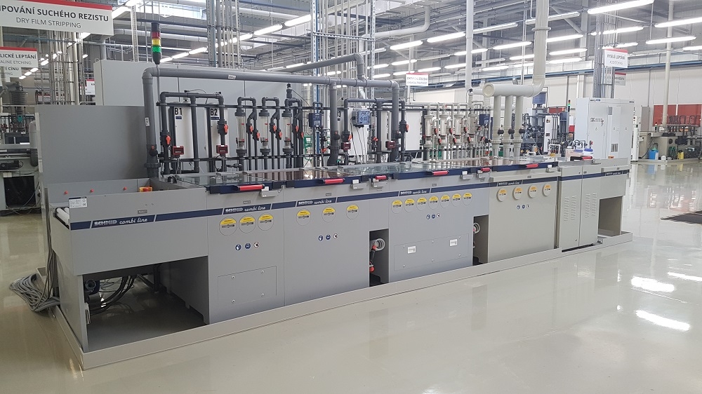
Schmid - copper pre-treatment
-Bond is suitable for treatment of internal layers before pressing. Unique surface topography formed by V-Bond improves adhesion of resin to copper.
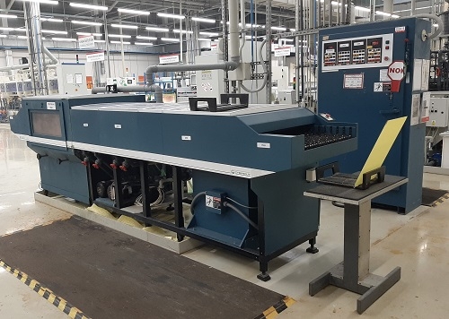
Cehmcu - tin stripper
Serves for removal of tin as protective resist before etching
Multilayer press
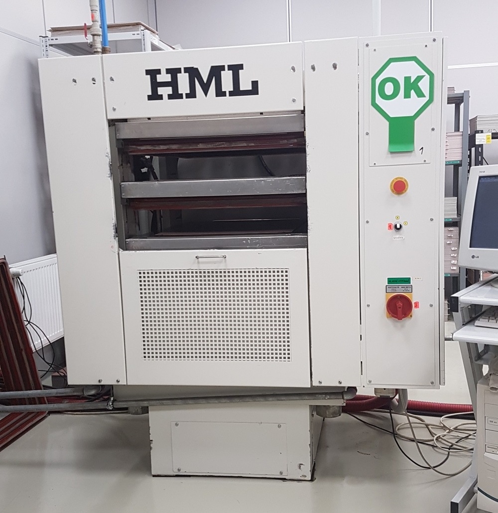
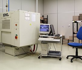
HML - multilayer press
Laminating hydraulic press HML LP-2000-V is a top double-deck press with a vacuum chamber. It is fully computer controlled with precise control of temperature and pressure parameters.
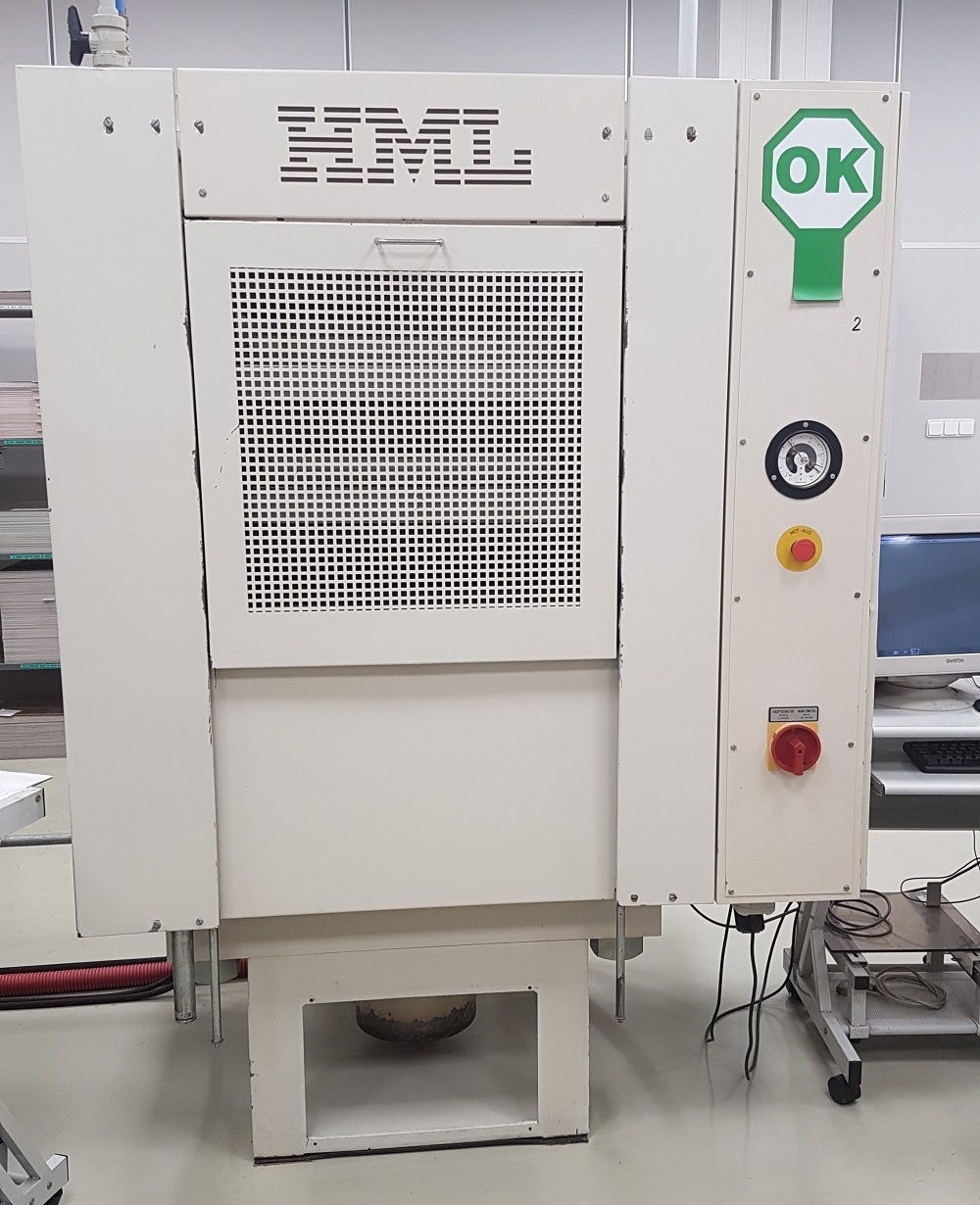
HML - multilayer press

Laminating hydraulic press HML LP-3000-V is a top three-deck press with a vacuum chamber. It is fully computer controlled with precise control of temperature and pressure parameters.
Surface finishing
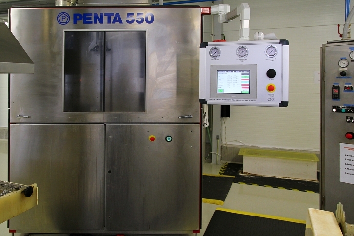
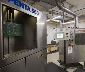
Penta - HAL lead free
A traditional PCB surface treatment that continues to find significant application despite its limitations is HAL (Hot Air Solder Levelling). Gatema PCB offers both HAL with lead solder (Pb37Sn63) and ROHS compliant tin solder (Sn99+). The solder is regularly regenerated and its composition is verified by OES directly at the supplier.
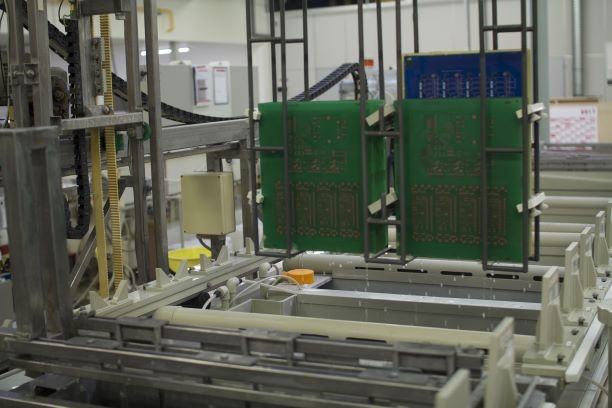
PPT - Immersion Silver
Immersion silver has best usage in HF applications. Because of missing Nickel is ideal for high frequency signals. Silver is better conductor than Au or Cu. It is easily solderable finish – IAg thickness is only 0,1 µm so even flatless is great. Silver is better conductor than Au or Cu. It is easily solderable finish – IAg thickness is only 0,1 µm so even flatless is great. Because of this characteristics it is commonly used for high construction classes of the printed boards too.
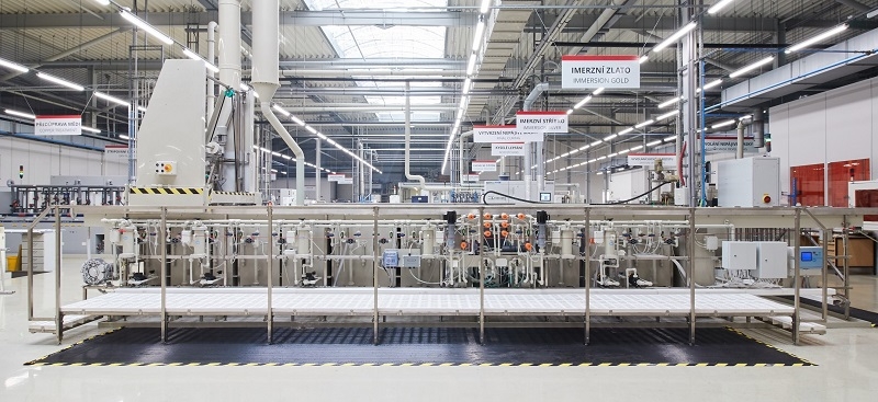
PPT Trenčianská Teplá - ENIG
Gold is an ideal element for top PCB cover. Given that gold doesn´t form oxides, the temperature and storage conditions have nearly no effect on its durability or condition compared to other finishes. Excellent adhesion is result of practically instant dissolution of gold into the solder. Nickel layer needs to be coated between copper and gold layers to prevent their mixing and therefore causing problems with soldering. This finish is suitable for AI wire bonding.
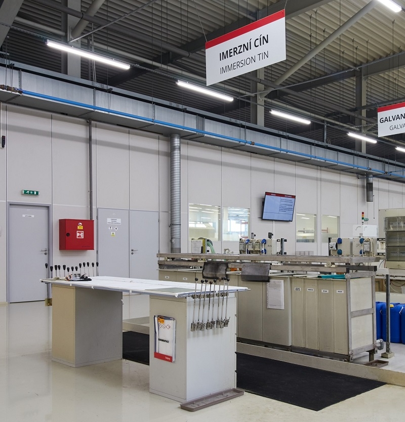
PPT Trenčianská Teplá - chemical tin

Chemical tin bath excludes thin and even layer of pure tin selectively on copper surface and in plated holes. Tin layer acquired by this process meets all modern final PCB´s finish requirements.
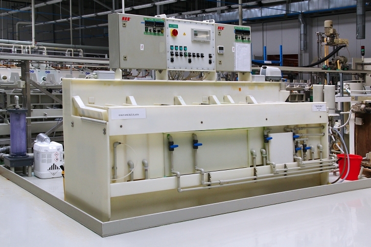
PPT Trenčianská Teplá - galvanic Ni/Au
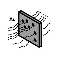
During the process is applied cca 5-10 um of glavanic nickel and 1-3 um of galvanic gold. In this case we talk about so-called hard gold. Galvanic gold is mostly used for protection from direct contact of connectors.
Testing
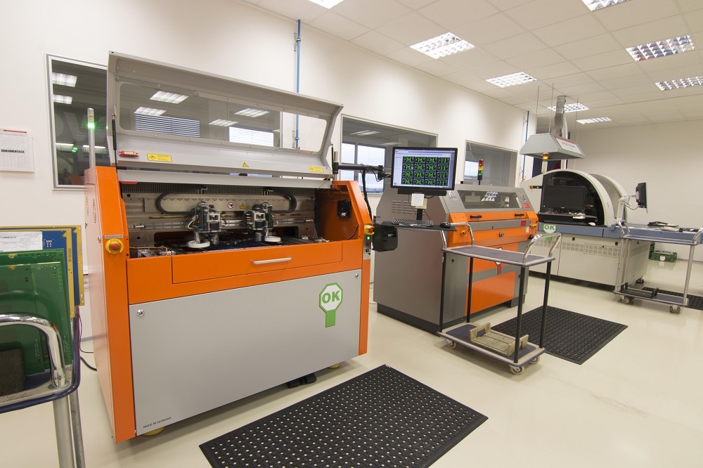
Electric testing
Electric testers ATG A5 XL8 / A3*8 / A7 are top equipment for testing of not assembled PCB. Tester has 8 probes in total which perform parallel contacting and measurement of boards. Customer shall receive certificate that guarantees reliability of supplied goods with each delivery of tested printed circuit boards.
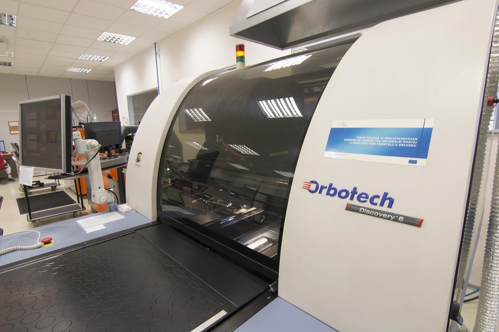
Orbotech - AOI
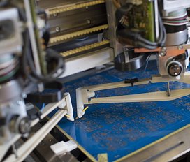
AOI automated optical inspection system based on comparison of CAM software output data and real PCB image. Camera system verifies in real time possible short-circuit, open-circuit on surface , further it is able to evaluate etching level which does not meet IPC standard parameters etc.
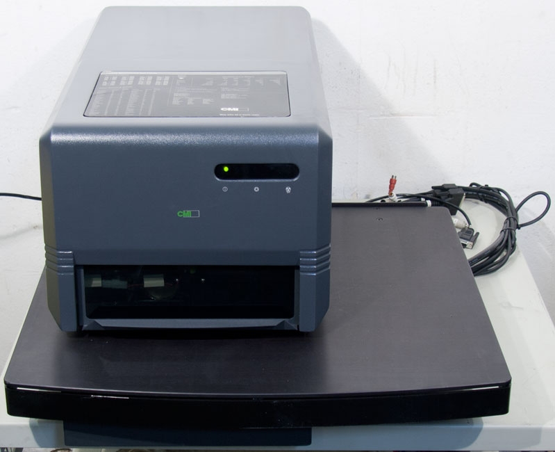
Oxford Instruments - X-ray analyzer
CMI 900 is designed for non-destructive measurement of the thickness of the surface layers. These analyzers are able to measure thickness of any surface, single/multi layers or alloys on almost any underlay. Device is also able determine concentration of solution, composition of alloys and perform analysis of materials.
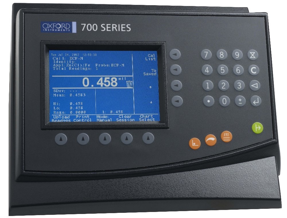
Oxford Instruments - copper thickness measurement

CMI 700 is modular device for exact determination of the thickness of different layers of Cu both on surface and in holes. Device can be configured in any combination with three measuring modules: micro-resistance module MRX, Beta backscatter module and module based on principle of eddy currents and magnetic induction EMX.
Neutralization
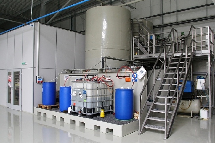
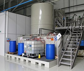
Neutralization

Neutralization station deals with water waste created by production´s chemical processes. Gatema has an automatic neutralization with capacity of 75 m³ a day. Water waste is pumped from accumulation tank into the assembly of three cascaded flow reactors. After this filtration the waste is drained into sedimentation reactor where sludge is sediment and separated water is drained into the sewerage. Sludge is pumped into the special reactor from where by air-membrane pump is pressed to hydraulic sludge presser. Neutralization station is equipped with a recording flowmeter and water left the station through recording PH control probe.

