
Wet processes
These lines are used for chemical treatment of semi-finished and finished plates. Processes include induction, etching, mechanical and chemical cleaning, surface pretreatment and activation and, most importantly, electroplating. Wet processes ensure the cleanliness and quality of the inner layers in particular and contribute significantly to the durability of the plate.
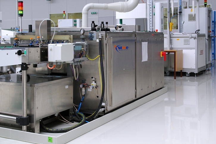

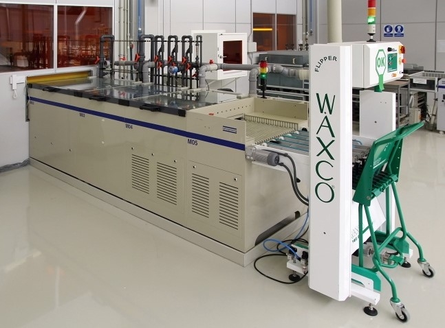
WISE - brushing
Within the PCB production a brushing line is used for removal of burr from holes and oxidation from copper surfaces. The line is equipped with an automatic brush pressure setting and high pressure rinsing. Of course there is a filtration system for brushes and rinses.


Plasonic - plasma
Plasma treatment removes resin from walls of drilled holes to allow perfect connection of galvanic copper on PCB internal layers. This method is convenient either for standard FR4 materials and for advanced materials with higher Tg, halogen free, polyimide (flex, rigid-flex), PFE etc. as well
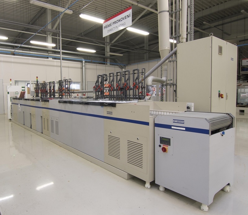

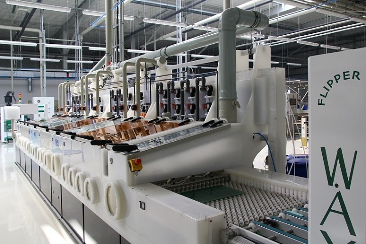
Laif - direct plating
The process of direct plating is based on graphite layer deposit on PCB dialectric surface which are to be plated through with galvanic copper. It is essential process verified by long-term operation.

Matusewitz - chemical cleaning
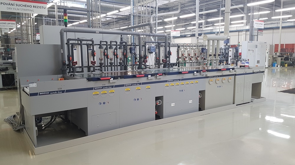
Matusewitz MECetch line – this process replaces the brushing process in some areas. Matusewitz MECetch line – this process replaces the brushing process in some areas. It brings far greater copper roughness and therefore it´s bigger surface. This treatment is suitable for application with dry resist, solder mask even for finishes pre-treatment. This technology is used also for copper surface treatment for flexi PCBs thanks to its minimal mechanical stress. Modern line software enables flexible program setting and simultaneously controls the automatic dosing based on continuous copper measurement.

Laif - resist developer
After dry resist exposure future connections are developed. This means that not imaged areas of photo sensitive material are chemically removed in sodium carbonate solution.
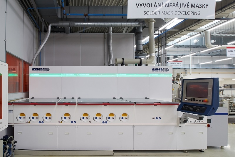

Schmid - solder mask developer
Not imaged surfaces of solder mask are removed by developing process. These are the places to which the customer can later solder.
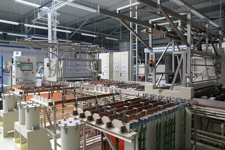

PPT Trenčianská Teplá - galvanic line
Galvanic line serves for plating-through of holes and copper thickening to required thickness and it represents core process of PCB production. The line contains acid copper and galvanic tin baths.

Wise - dry resist stripper
The new line, from the Italian company WISE, is equipped with an automatic mode of control and dosing of chemicals.

Schmid - acid etching
Excess copper is removed from PCB by using copper dichloride solution. The system itself measures bath selected parameters and upon results adds necessary chemicals.
Laif - alcalic etching
Ammoniacal etchant removes excess copper from PCB. The process itself controls solution pH value and density.

Schmid - copper pre-treatment
-Bond is suitable for treatment of internal layers before pressing. Unique surface topography formed by V-Bond improves adhesion of resin to copper.

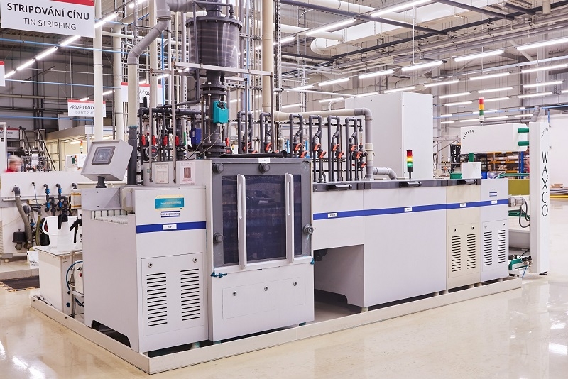
Cehmcu - tin stripper
Serves for removal of tin as protective resist before etching

Plugging
For filling holes, we utilize technology from I.T.C., which can fill blind vias using two heads. We fill the boards according to IPC 4761, type VII. The holes are plated with copper and finished with a final surface treatment. This technology allows for via-in-pad.


